- 您现在的位置:买卖IC网 > Sheet目录369 > W9751G6IB-25 (Winbond Electronics)IC DDR2-800 SDRAM 512MB 84-WBGA
�� �
�
�W9751G6IB�
�7.3.8�
�Self� Refresh� Exit� Command�
�(CKE� =� "H",� CS� =� "H"� or� CKE� =� "H",� CS� =� "L",� RAS� =� "H",� CAS� =� "H",� WE� =� "H",� BA0,� BA1,�
�A0� to� A12� =� Don’t� Care)�
�The� procedure� for� exiting� Self� Refresh� requires� a� sequence� of� commands.� First,� the� clock� must� be�
�stable� prior� to� CKE� going� back� HIGH.� Once� Self� Refresh� Exit� is� registered,� a� delay� of� at� least� t� XSNR�
�must� be� satisfied� before� a� valid� command� can� be� issued� to� the� device� to� allow� for� any� internal� refresh�
�in� progress.� CKE� must� remain� HIGH� for� the� entire� Self� Refresh� exit� period� t� XSRD� for� proper� operation�
�except� for� self� refresh� re-entry.�
�Upon� exit� from� Self� Refresh,� the� DDR2� SDRAM� can� be� put� back� into� Self� Refresh� mode� after� waiting�
�at� least� t� XSNR� period� and� issuing� one� refresh� command� (refresh� period� of� t� RFC� ).� NOP� or� Deselect�
�commands� must� be� registered� on� each� positive� clock� edge� during� the� Self� Refresh� exit� interval� t� XSNR� .�
�ODT� should� be� turned� off� during� t� XSRD� .�
�The� use� of� Self� Refresh� mode� introduces� the� possibility� that� an� internally� timed� refresh� event� can� be�
�missed� when� CKE� is� raised� for� exit� from� Self� Refresh� mode.� Upon� exit� from� Self� Refresh,� the� DDR2�
�SDRAM� requires� a� minimum� of� one� extra� auto� refresh� command� before� it� is� put� back� into� Self� Refresh�
�mode.�
�7.3.9�
�Refresh� Command�
�(� CS� =� "L",� RAS� =� "L",� CAS� =� "L",� WE� =� "H",� CKE� =� "H",� BA0,� BA1,� A0� to� A12� =� Don’t� Care)�
�Refresh� is� used� during� normal� operation� of� the� DDR2� SDRAM.� This� command� is� non� persistent,� so� it�
�must� be� issued� each� time� a� refresh� is� required.�
�The� refresh� addressing� is� generated� by� the� internal� refresh� controller.� This� makes� the� address�
�bits� ”Don’t� Care”� during� an� Auto� Refresh� command.� The� DDR2� SDRAM� requires� Auto� Refresh� cycles�
�at� an� average� periodic� interval� of� t� REFI� (max.)� .�
�When� the� refresh� cycle� has� completed,� all� banks� of� the� DDR2� SDRAM� will� be� in� the� precharged� (idle)�
�state.� A� delay� between� the� auto� refresh� command� (REF)� and� the� next� activate� command� or�
�subsequent� auto� refresh� command� must� be� greater� than� or� equal� to� the� auto� refresh� cycle� time� (t� RFC� ).�
�To� allow� for� improved� efficiency� in� scheduling� and� switching� between� tasks,� some� flexibility� in� the�
�absolute� refresh� interval� is� provided.� A� maximum� of� eight� Refresh� commands� can� be� posted� to� any�
�given� DDR2� SDRAM,� meaning� that� the� maximum� absolute� interval� between� any� Refresh� command�
�and� the� next� Refresh� command� is� 9� x� t� REFI� .�
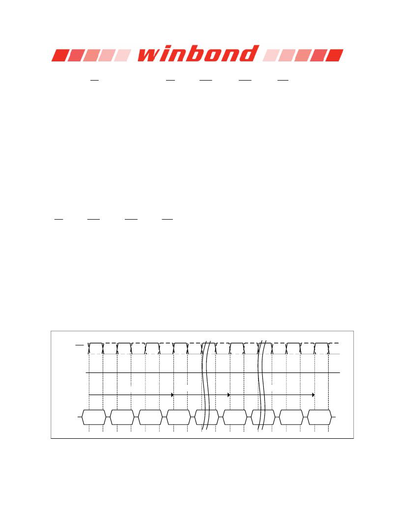
�T0�
�T1�
�T2�
�T3�
�Tm�
�Tn�
�Tn� +� 1�
�CLK/CLK�
�CKE�
�"HIGH"�
�≧� tRP�
�≧� tRFC�
�≧� tRFC�
�CMD�
�Precharge�
�NOP�
�NOP�
�REF�
�REF�
�NOP�
�ANY�
�Figure� 13� —� Refresh� command�
�Publication� Release� Date:� Oct.� 23,� 2009�
�-� 22� -�
�Revision� A06�
�发布紧急采购,3分钟左右您将得到回复。
相关PDF资料
W9751G6KB-25
IC DDR2 SDRAM 512MBIT 84WBGA
W9812G6JH-6I
IC SDRAM 128MBIT 54TSOPII
W9816G6IH-6I
IC SDRAM 16MBIT 50TSOPII
W9825G6JH-6I
IC SDRAM 256MBIT 54TSOPII
W9864G6JH-6I
IC SDRAM 64MBIT 54TSOPII
WM-5614
CABINET WALL MOUNT 37.25X17.9"
WRR-2244
RACK WALL MOUNT RELAY 42" X 19"
WRR-2264
RACK WALL MOUNT 75.25" X 19"
相关代理商/技术参数
W9751G6JB
制造商:WINBOND 制造商全称:Winbond 功能描述:8M ? 4 BANKS ? 16 BIT DDR2 SDRAM
W9751G6JB-25
制造商:Winbond Electronics Corp 功能描述:512GB DDRII
W9751G6JB-3
制造商:Winbond Electronics Corp 功能描述:512MB DDRII
W9751G6KB
制造商:WINBOND 制造商全称:Winbond 功能描述:8M ? 4 BANKS ? 16 BIT DDR2 SDRAM
W9751G6KB-18
制造商:Winbond Electronics Corp 功能描述:IC MEMORY
W9751G6KB-25
功能描述:IC DDR2 SDRAM 512MBIT 84WBGA RoHS:是 类别:集成电路 (IC) >> 存储器 系列:- 标准包装:1 系列:- 格式 - 存储器:闪存 存储器类型:闪存 - NAND 存储容量:4G(256M x 16) 速度:- 接口:并联 电源电压:2.7 V ~ 3.6 V 工作温度:0°C ~ 70°C 封装/外壳:48-TFSOP(0.724",18.40mm 宽) 供应商设备封装:48-TSOP I 包装:Digi-Reel® 其它名称:557-1461-6
W9751G6KB25A
制造商:WINBOND 制造商全称:Winbond 功能描述:Double Data Rate architecture: two data transfers per clock cycle
W9751G6KB25I
制造商:Winbond Electronics Corp 功能描述:DRAM Chip DDR2 SDRAM 512M-Bit 32Mx16 1.8V 84-Pin WBGA 制造商:Winbond Electronics Corp 功能描述:IC DDR2 SDRAM 512MBIT 2.5NS BGA